

Fourth-generation semiconductor ushered in new progress related A-share companies to seize the "new wind mouth"
发布时间 : 2024-01-10
In recent years, scientific and technological innovation, which has been repeatedly "classified as a key point", has become the main battlefield of the international scientific and technological strategy game. Among them, technological breakthroughs in the field of semiconductors are the international science and technology strategy must contend for heights. In this context, gallium oxide, which is regarded as one of the best materials for fourth-generation semiconductors, has entered people's vision and is expected to gradually become a new air outlet on the semiconductor circuit.
Behind the major breakthrough: China's gallium oxide industry continues to progress
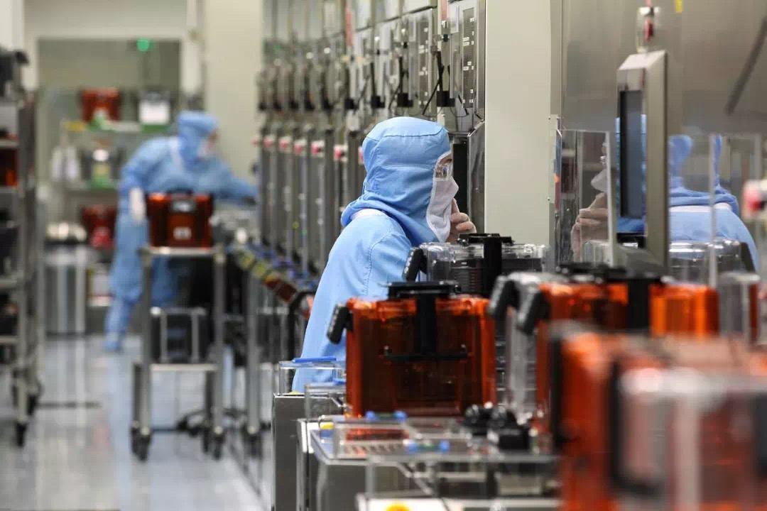
Professor Chen Haifeng's team at the Key Laboratory of New Semiconductor Devices and Materials at Xi 'an University of Posts and Telecommunications in China has successfully prepared high-quality gallium oxide epitaxial wafers on 8-inch silicon wafers, which marks an important progress in the research of ultra-wide band gap semiconductors at the school. In fact, China's research and development of gallium oxide industry has never stopped.
On February 28, it was reported that China Electronics 46 Institute successfully prepared China's first 6-inch gallium oxide single crystal, reaching the highest international level. Focusing on the direction of multi-crystal surface, large size, high doping, low defect, etc., the Gallium oxide team of the 46 Institute of China Electronics Engineering successfully constructed a thermal field structure suitable for 6-inch gallium oxide single crystal growth from the design of large-size gallium oxide thermal field, breaking through the 6-inch gallium oxide single crystal growth technology, and has good crystallization performance, which can be used for the development of 6-inch gallium oxide single crystal substrate.
On February 27, Professor Long Shibing's research group of the School of Microelectronics of the University of Science and Technology of China and the processing platform of Suzhou Nano Institute of the Chinese Academy of Sciences jointly developed a gallium oxide vertical trough gate field-effect transistor by using oxygen atmosphere annealing and nitrogen ion implantation technology, respectively. The relevant research results were published online in Applied Physical Communication and IEEE Electronic Device Communication.
It is precisely because of the improvement of attention and the increase of research and development efforts, in recent years, China has made breakthroughs in the preparation of gallium oxide, from 2 inches to 6 inches last year, and then to the latest 8 inches, gallium oxide preparation technology is becoming more mature.
What is the high-profile gallium oxide?
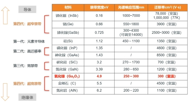
Gallium oxide is an inorganic compound, also known as gallium trioxide (Ga2O3), which is a wide band gap semiconductor. After the third generation of semiconductors based on silicon carbide and gallium nitride, gallium oxide is regarded as one of the best materials for the next generation of semiconductors.
The first generation semiconductor refers to silicon (Si), germanium (Ge) and other elemental semiconductor materials;
The second generation semiconductor refers to gallium arsenide (GaAs), indium phosphide (InP) and other semiconductor materials with high mobility;
The third generation semiconductor refers to silicon carbide (SiC), gallium nitride (GaN) and other wide band gap semiconductor materials;
Fourth-generation semiconductors refer to ultra-wide band gap semiconductor materials such as gallium oxide (Ga2O3), diamond (C), aluminum nitride (AlN), and ultra-narrow band gap semiconductor materials such as gallium antimonide (GaSb) and indium antimonide (InSb).
Figure: Semiconductor materials sorted by band gap width Source: Core list
As can be seen from the figure, compared with the third-generation semiconductor silicon carbide (SiC) and gallium nitride (GaN), the band gap of gallium oxide reaches 4.9eV, which is higher than that of silicon carbide (3.2eV) and gallium nitride (3.39eV). The wider band gap means that electrons need more energy to transition from the valence band to the conduction band. Therefore, gallium oxide has the characteristics of high pressure resistance, high temperature resistance, high power and radiation resistance. In addition, under the same specifications, wide band gap materials can manufacture devices with smaller die size and higher power density, saving supporting heat dissipation and wafer area, and further reducing costs.
Hao Yue, academician of the Chinese Academy of Sciences, clearly pointed out in an interview that gallium oxide material is one of the most likely to shine in the future, and in the next 10 years or so, gallium oxide devices may become competitive power electronic devices, which will directly compete with silicon carbide devices.
Gallium oxide looks to become a new air outlet of semiconductor circuit
In recent years, the demand for third-generation semiconductor materials, mainly silicon carbide and gallium nitride, has exploded and become the object of the capital market. Today, the shining debut of the fourth-generation semiconductor materials represented by gallium oxide is expected to become A new outlet of the semiconductor circuit, and relevant A-share companies have also been prepositioned.
According to statistics, there are still few enterprises engaged in the research and development of gallium oxide in China, among which the enterprises involved in the business of A-shares mainly include Xinhu Hubao, A Shi Chuang, Nanda Optoelectronics, aerospace electronics and so on.
New Zhonghu Bao: The invested Fujia Gallium Industry focuses on the research and development of fourth-generation semiconductor materials with wide bandgap semiconductor gallium oxide materials. At present, it has initially established full-link research and development capabilities of gallium oxide single crystal material design, thermal field simulation, single crystal growth, wafer processing, etc., and has launched gallium oxide UID (unintentionally doped), conductive and insulating products with specifications of 2 inches and below.
Ashtron: Target products of gallium oxide and gallium oxide mixtures can be customized for customers according to their needs.
Nanda Optoelectronics: is the world's main MO source supplier, some products can be used for the preparation of gallium oxide.
Aerospace Electronics: The wholly-owned subsidiary Times Minxin Company is carrying out technical research and layout in the field of gallium oxide.
