

The world's first! China's chip field has made a major breakthrough!
发布时间 : 2023-12-18
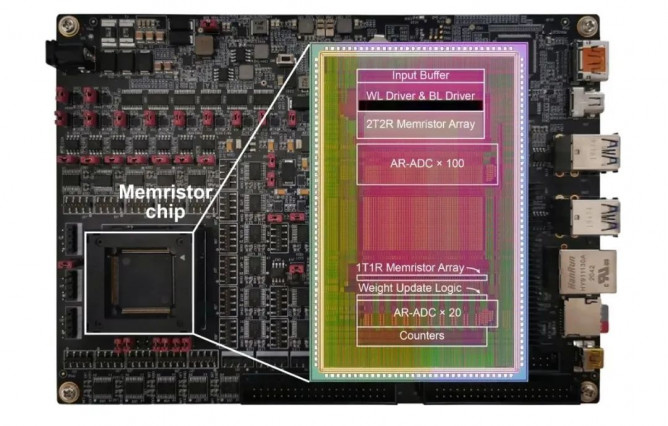
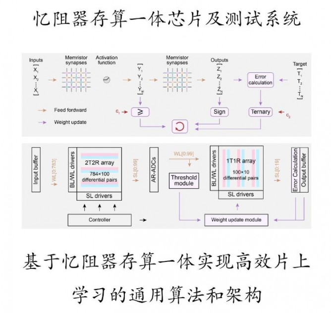
Recently, the team of Professor Wu Huaqiang and Associate Professor Gao Bin of the School of Integrated Circuits of Tsinghua University developed the world's first full-system integration, supporting efficient on-chip learning (machine learning can be directly completed at the hardware end) memristor memory and computing integrated chip based on the integrated computing paradigm, and made a major breakthrough in the field of memristor memory and computing integrated chip supporting on-chip learning. It is expected to promote the development of artificial intelligence, autonomous driving wearable devices and other fields. The results are published online in the latest issue of Science.
At present, the relevant international research mainly focuses on the demonstration of learning function at the level of memristor array. However, the realization of full-system integrated memristor chip supporting efficient on-chip learning still faces great challenges and has not been realized so far, mainly because the high-precision weight updating method required by traditional backpropagation training algorithm has poor adaptability to the actual characteristics of the memristor.
It is understood that facing the major challenges of traditional storage separation architecture that restricts computing power improvement, Wu Hua Qiang and Gao Bin creatively proposed adapting memristor storage and computing to achieve a new general algorithm and architecture for efficient on-chip learning (STELLAR), and effectively realize the monolithic three-dimensional integration of large-scale analog memristor arrays and CMOS. Through the collaborative innovation of the whole process of algorithm, architecture and integration mode, the world's first memory and computing integrated chip of memristor supporting efficient on-chip learning is developed.
The chip contains all the circuit modules necessary to support complete on-chip learning, and successfully completes a variety of on-chip incremental learning function verification such as image classification, speech recognition and control tasks, demonstrating high adaptability, high energy efficiency, high versatility, and high accuracy, effectively strengthening the learning and adaptation ability of intelligent devices in practical application scenarios. Under the same task, the energy consumption of the chip to achieve on-chip learning is only 3% of that of the application-specific integrated circuit (ASIC) system under the advanced process, showing excellent energy efficiency advantages and great application potential to meet the needs of high computing power in the era of artificial intelligence, providing an innovative development path to break through the energy efficiency bottleneck under the traditional von Neumann computing architecture.
// Tsinghua University has made important progress in the research and development of ultra-high sensitivity photoresist //
Photoresist is a key material for large-scale manufacturing of integrated circuit chips. After the development of deep ultraviolet (DUV) and extreme ultraviolet (EUV) lithography, the sensitivity of photoresist to light source is insufficient, which greatly increases the difficulty and cost of manufacturing the lithography machine and its supporting light source. Recently, the new energy and materials chemistry team of the Institute of Nuclear Energy and New Energy Technology of Tsinghua University combined the efficient thiol-ethylene click chemistry technology with multi-functional metal oxide nanocluster photoresist technology, and proposed a new idea and new method of "click lithography" for the first time in the world, and successfully produced ultra-high sensitivity photoresist samples. The lithography test results of international authorities show that this material can achieve high contrast imaging at very low exposure doses. The maximum sensitivity in deep UV lithography is 7.5 mJ cm-2, which reduces the required exposure dose by about 20 times compared with the traditional photoresist system.
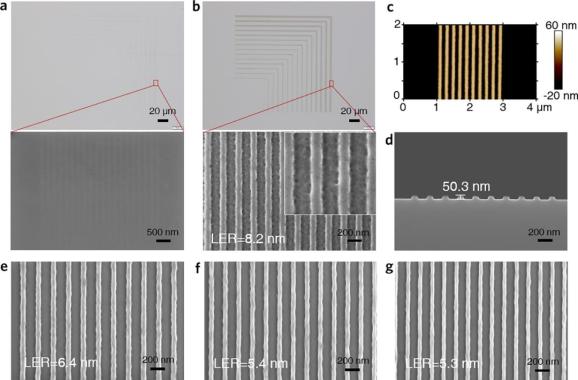
At the same time, dense patterns with a linewidth resolution of 45nm were obtained by low-dose electron beam lithography (10-40 μC cm-2), demonstrating its ability to be applied to high-resolution lithography. Then the author also made a preliminary study on the post-processing properties, etching resistance and pattern transfer ability of the photoresist based on click reaction.
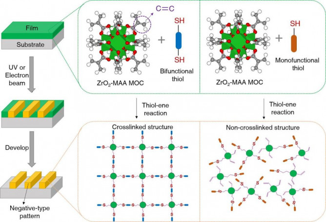
Figure 1. Schematic diagram of click lithography strategy
Figure 2. Click the lithography result
The research results can not only strongly support the development of new high-efficiency photoresist, but also is expected to bring about major changes in the design, manufacturing and operation of the lithography machine and its supporting light source system, greatly reducing the difficulty and cost, and may open up a new track of lithography machine technology, and have a far-reaching impact on the technological progress and industrial development of integrated circuits. The technology could also play a major role in other areas of efficient, high-precision nanofabrication.
the findings are published in the Journal of the American Chemical Society under the title "Exceptional Light Sensitivity by Thiol-ene Click Lithography. American Chemical Society.
The co-corresponding authors of the paper are Associate Professor Xu Hong and Researcher He Xiangming, Laboratory of New Energy and Materials Chemistry, Institute of Nuclear Energy and New Energy Technology, Tsinghua University. The first author is Wang Qianqian, postdoctoral fellow, Tsinghua University. The research was supported by the National Natural Science Foundation of China, the Beijing Science and Technology Commission and the independent research project of Tsinghua University. The High Performance Computing Center of Tsinghua University provided computing resources.
Prev: Xiaomi, Ov new products, domestic CMOS manufacturers fight 50M
Next: Huawei Dubai released the first open headphones for 199 euros, and added high-end to compete with Apple and Samsung
